DATE OF BIRTH PROJECT
Project Overview:

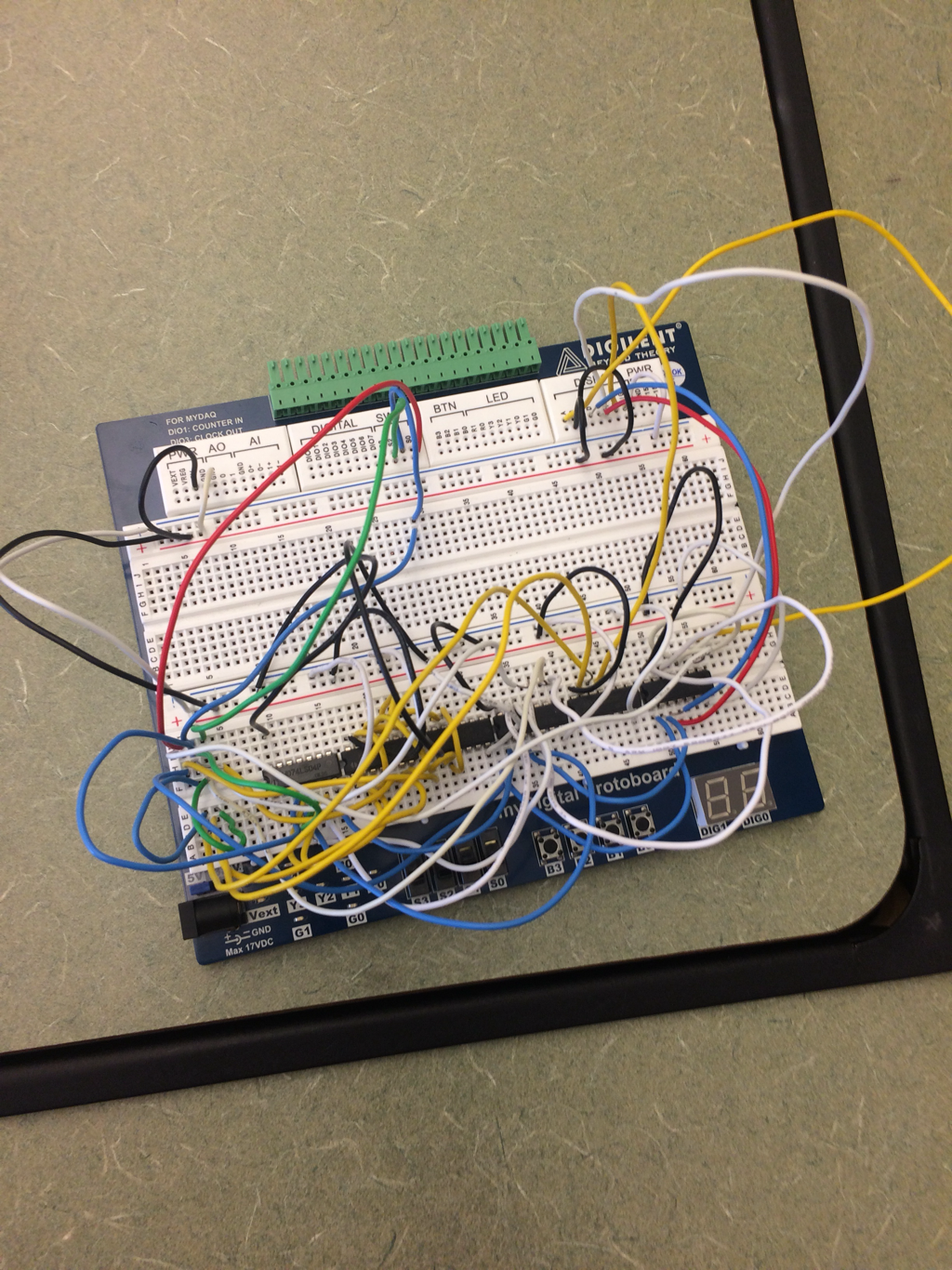
This picture above is the last stage of the building, it is also the same picture before this picture.
|
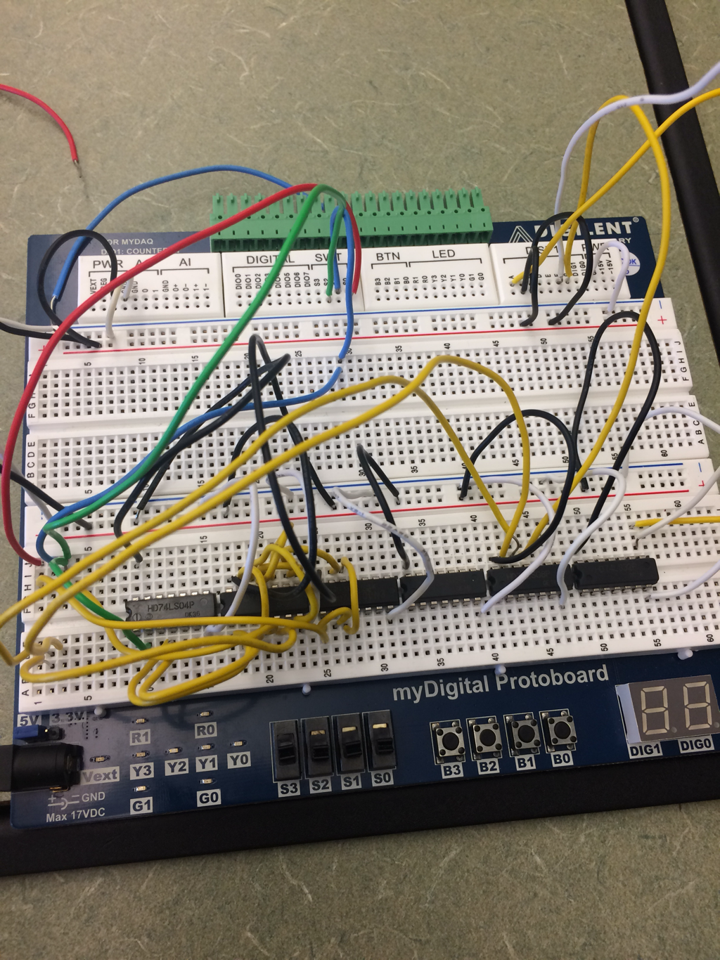
This is the second stage of building the circuit where I put in the inputs and created the NAND segment for A in the motherboard.The yellow is the NAND segment and the other colors are the X,Y, and Z inputs.
|
|
The circuit that is being designed (shown to the left) is supposed to show your birthday when you input specific combinations of inputs.
|
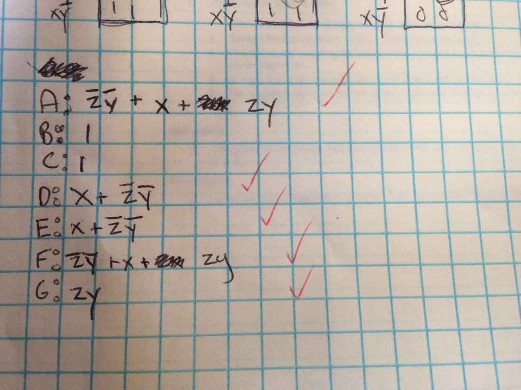
Truth table
The truth table is basically the circuit but written down on paper in the form of numbers. It also allows you to create a logic expression or create k-maps.
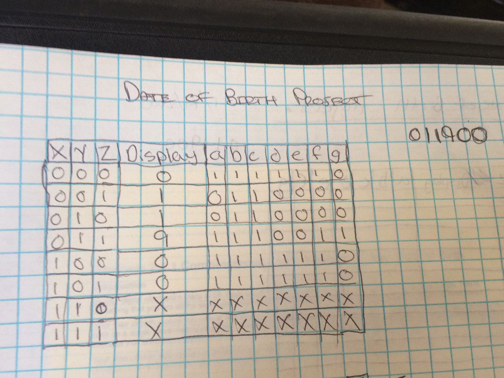
The A through G columns are there to represent the lights in the display so there are a total of 7 lights creating the display that form together to create specific numbers and a few letters and in a clockwise rotation starting from the top the letters go from A to B to C and so on to the letter G. The X means that the output that is given when the specified inputs are put it, the outcome doesn't matter.
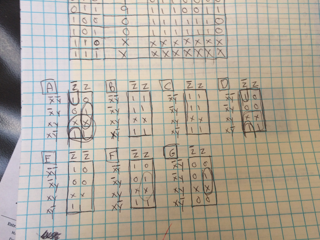
K-Maps and simplified logic expressions
|
|
K-mapping works by grouping together the most 1's or X's as possible in an even number. So you can group them in rows of 2 or 4, a square of 4, or you could do a PAC MAN thing and circle 1's in adjacent corners or all four corners if there are either 1's or X's in those corners. You can't do it with zeros unfortunately, what would be the point then? And to fill in the table I did it by counting the 1's and 0's for a through g and numbering those 1's and 0's 1 through 8. Then I put those numbers in the k-map going from left to right 1-2 then 3-4 then 7-8 and 5-6. And no the 7-8 before the 5-6 is supposed to be there I don't know why, it just is. The expressions are in Sums of Products form because it is easier for me to do. To get the min terms after you would do the grouping in the k-mapping you would then look at the letters above see which ones cancel out and the write the ones that don't cancel out using Boolean theorems. And I did that for each of the 7 k-maps to get the min terms. It doesn't take very long either, it looks like it would but I assure you it does not. Why would I use k-mapping? I used it because it creates the already simplified logic expression when other technics create the un-simplified logic expressions which you then have to simplify, so it's faster. And it was a requirement but that's just a small reason.Why do I have so many expressions? Each expression represents one light in the display that would light up when I input the correct sequence of 1's and 0's. It is complicated because the one light has to turn and for multiple different sequences and not just one. That would be too easy.
MultiSim implementation
The picture below is the digital form of the circuit that will be used to create the date of birth mother board circuit.
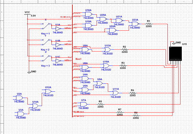
TThe circuit above is luckily in bus form. How do I know? Well the long bold red line going down the center is called a bus, so it's in bus form. 3 Inverter Gates, 5 AND Gates, 4 OR Gates, and 6 NAND Gates are required to build the circuit. Which means 1 Inverter chip (74LS04), 2 AND chips (74LS08), 1 OR chip (74LS32), and 2 NAND chips (74LS00) and need to build the circuit on the mother board. I decided to use NAND Gates on the A segment because it was the longest segment and I wanted to try it out and see what happens. NAND chips are able to create inverter, AND, and OR Gates based on the combination that they are put in, so they allow you to save specific chips by only using one type of chip for multiple different Gates.The same applies for a NAND and a NOR circuit, it saves you a lot of chips that would be normally needed and wasted to build a circuit. Unfortunately my NAND Gate had more Gates need then the original circuit designed for A, however the original design had 2 types of Gates and would have forced me to use a second OR Chip which would be wasting that chip. So even though it had more Gates it saved me in using more OR Gates on my mother board. It was also a requirement but once again that's a small detail. For the seven segment display I used a Common Cathode which you can tell by looking at the picture because the display is connected to ground and not power. ( A common Anode is connected to the power or VCC while the common Cathode is connected to the ground and not the power.) I used the Cathode because I believed it to be easy to use.The resistors are there to help manage power going into the display and to make sure that the display doesn't explode, cause that would be bad in my opinion.
Bill of materials
On this circuit I used two AND chips (74LS08), 2 NAND chips (74LS00), 1 OR chip (74LS32), and 1 inverter chip (74LS04). I also used in total about 60-70 wires for the whole finished circuit.
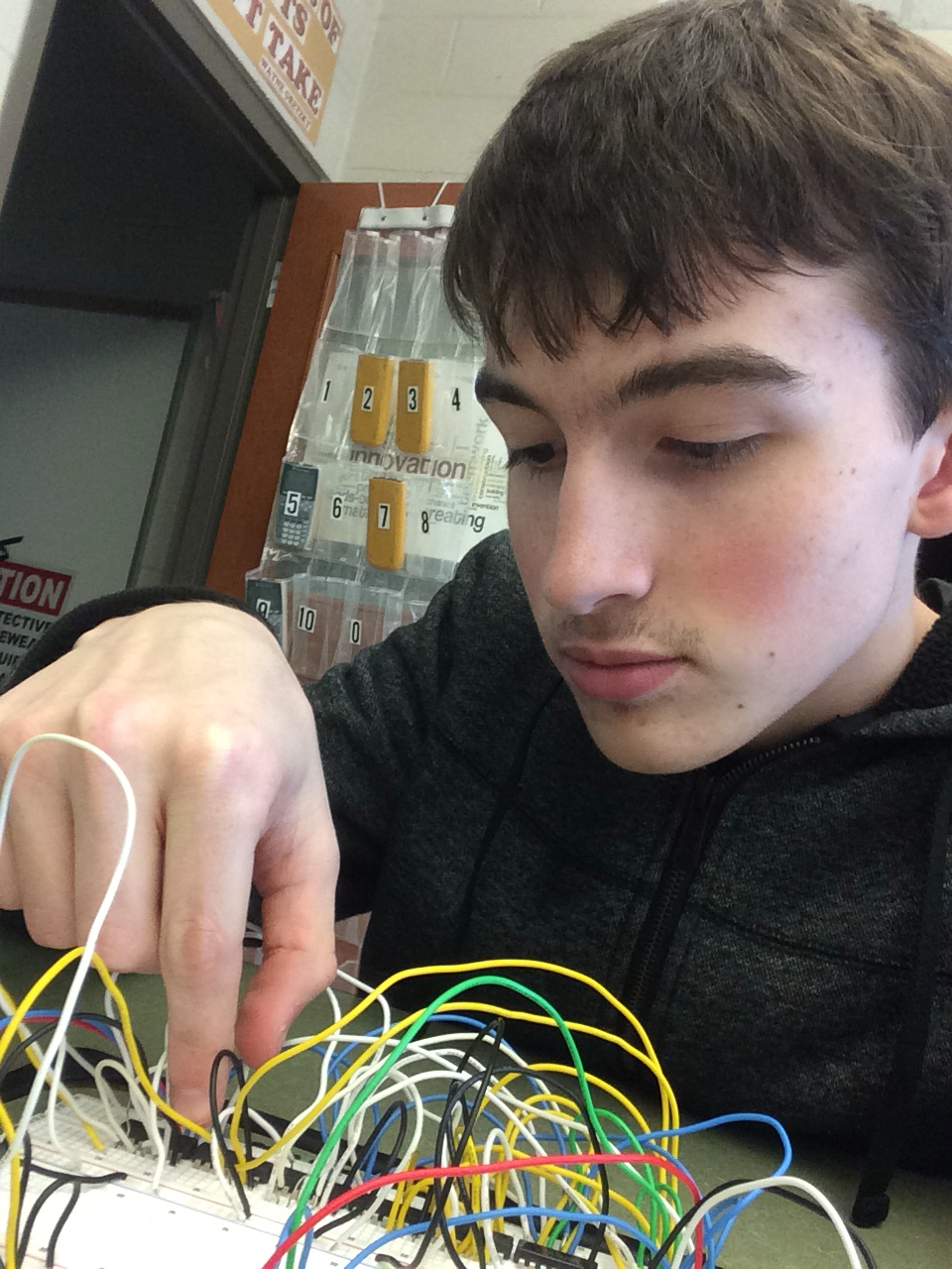
Bread-boarding
The picture above is the final working and simplified circuit of the diagram created in the previous sections on MultiSim.
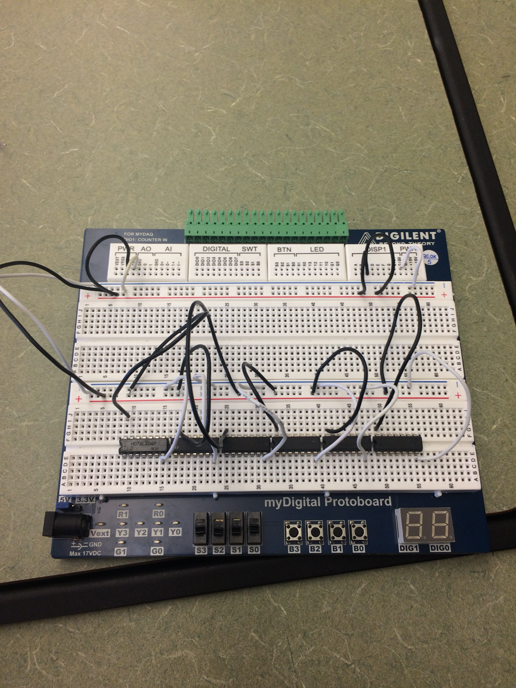
This is the first stage of building where I attached the ground and power to each chip. The power being black and the ground being white.
Conclusion
While doing this project I sort of got a behind the scenes view or what is happening with most digital equipment today. Such as some clocks using circuits like the one we built in this project. If I was to do something differently next time it would be to get everything down before I go on a college visit, since I wasn't down when I went on a recent college visit and it really messed up my schedule of trying to get this done along with every other project. What I still want to know is how complex can these types of circuits become in the real world and who builds them as a job? K-Mapping is useful because it can give you a simplified logic expression the first time instead of getting the in-simplified logic expression and then having to simplify the logic expression again which takes up more time. But overall I believe that this was a fun project to do, looking past the scheduling problems.
